by John Walt Childers, IPC-CID, Founder of Golden Gate Graphics

Formerly known as

GLOSSARY of Printed Circuit Design and Manufacturing

This glossary has key terminology in use in PCB design and manufacturing, with a smattering of electronics. The definitions were chosen so that their context would likely apply to reading material encountered by a PCB designer. Therefore, many of these terms will have other meanings not given here. It is recommended by scholars that you also clear up the non-technical definitions in regular dictionaries. There are such dictionaries recommended below.

This collection of terms came about as I, a PCB designer, ran across words and acronyms in my field for which meanings were hard to find. As I tracked them down, I made them part of this glossary. If you are a PCB designer, then this glossary could be a good place to start when you find a need to look up the meanings of words related to printed circuits or electronics.

Al­pha­bet­iz­ing Me­thod

Terms that begin with a symbol or a digit are placed in the SYMBOLS page. Terms that contain digits within them are alphabetized as if the numeric characters were spelled in English.

Terms with two or more words are alphabetized "dictionary style." They are alphabetized as though the spaces between the terms have been removed.
   If there are other characters in the term, such as a slash (/), dash (-) or plus sign (+), these are treated the same as spaces and ignored for the purpose of alphabetizing.

Click for Pronunciation Key


References and Dic­tio­nar­ies

Modern Dic­tio­nary of Elec­tron­ics by Rudolf F. Graf

This is the best, most usable dictionary for electronics, because its definitions help you grasp the terms and therefore the subject. Lesser dictionaries define electronics terms with even more difficult technical jargon, leading one into endless"word chains." Not this one.
You can buy the Modern Dictionary of Electronics new or used via the Internet.

Citation:
Graf, Rudolf F. Modern Dictionary of Electronics. Newnes, 1999.


The Random House Dic­tio­nary of the Eng­lish Lan­guage, Un­a­bridged, 2nd E­di­tion

You need a big, comprehensive dictionary. Get this one. Despite being a big dictionary, The Random House has great definitions, quick to grasp.

Although out of print, as of 2022 you could still buy a great used copy online for $40 including shipping or possibly for much less. Two versions are available of the 2nd Edition, Unabridged:

I have no idea what the difference is for the deluxe edition, but there seem to be fewer copies of it available in 2020 than the regular edition. I'm sure they both have the same set of definitions. My copy has both ISBNs listed in the front matter, and it is the regular edition.

Citation:
Flexner, Stuart Berg, and Leonore Crary Hauck, editors. The Random House Dictionary of the English Language. Unabridged, 2nd Edition, Random House, 1987.
Our Customer Testimonials
Golden Gate Graphics in an official Altium Service Bureau
Golden Gate Graphics is an official Altium Service Bureau

Example Printed Boards

Click for Examples of PCBs designed by Golden Gate Graphics
Articles by the Founder

K Terms Index

GLOSSARY of Printed Circuits

Symbols A B C D E F G H I J K L M N O P Q R S T U V W X Y Z

On mobile phones, scroll down or click to access K Terms Index

Arrow pointing up, clicking will move to top of page.K

Index to terms on this page:

KBC Kelvin connection Kelvin double bridge

Arrow pointing up, clicking will move to top of page.
­

KBC — KeyBoard Controller

K Terms Index ­

Kelvin connection  — (KEL-vin kən-NEK-shən) Pronunciation Key

  1. noun [PCB Layout] An electrical connection that goes directly to a target component's terminals with no other connections along the same PCB trace.
     Delano_Cary_L_Designing_With_Switching_Amplifiers
  2.  
  3. noun [PCB Layout] A pair of connections on a PCB, which, in addtition to each one going directly to a target component's terminals with no other connections along the same PCB trace, are of equal length and equal trace width. They are often routed close together with an equal spacing, where possible.
     Kando_Bob_PCB_Layout_Guidelines_Power_Controllers
  4. A Kelvin connection is a four-wire method of making electrical contact to a component or circuit node that separates the current-carrying path from the voltage-sensing path. It ensures that resistance measurements or voltage readings are not distorted by the voltage drop in the test leads or contact resistance.

    This connection method exists so that any resistance in the leads or contacts which could add error to measurements is eliminated. In precision circuits and low-resistance measurements, such parasitic drops can produce substantial inaccuracies, prompting the need for a separate sense pair with negligible current flow.

The result of using a Kelvin connection is a far more accurate representation of the true voltage across a device under test, independent of lead or contact resistance. This improves measurement fidelity in resistance metering, current sensing, and PCB test fixtures, especially when measuring shunts, vias, or plated traces carrying significant current.

A Kelvin connection can be influenced or improved by careful physical layout: routing the sense lines close and parallel to the current-carrying lines, minimizing loop area and noise pickup, and ensuring symmetrical contact points at the component terminals. On printed circuit boards, dedicated pads or vias for sense lines can be added at the precise measurement locations.

The term originates from Lord Kelvin (William Thomson, 1824–1907), the British physicist and electrical engineer who established the principles of absolute temperature and electrical measurement precision. His name became associated with this technique because of his contributions to accurate resistance measurement and the development of the Kelvin double bridge.


K Terms Index
Arrow pointing up, clicking will move to top of page.

Kelvin double bridge — (KEL-vin DUB-uhl brij) Pronunciation Key noun [Electrical Measurement, Metrology, Precision Instrumentation]

A Kelvin double bridge is a precision electrical circuit used to measure very low resistances with high accuracy by eliminating the effects of lead and contact resistances. It extends the principle of the Wheatstone bridge by incorporating an additional set of ratio arms and a second pair of potential leads, thereby maintaining a true four-terminal configuration for the unknown resistor.

This circuit exists to solve the problem that arises in low-resistance measurement: even small resistances in the connecting leads or contacts can produce voltage drops comparable to or larger than those across the test specimen itself. The Kelvin double bridge was designed to cancel these unwanted resistances by using separate current and potential paths, ensuring that the voltage measurement depends solely on the unknown resistance.

The result of employing a Kelvin double bridge is the ability to measure resistances in the micro-ohm range with exceptional accuracy, a capability essential for testing materials, shunt resistors, and conductive traces where minimal voltage drop must be verified. Its design principles form the basis for modern four-wire ohmmeters and automated resistance-measurement systems used in laboratories and high-reliability manufacturing environments.

The accuracy of a Kelvin double bridge can be influenced by the precision of its ratio arms, the stability of its standard resistor, and the balance sensitivity of its galvanometer. Improvements can be achieved through temperature-compensated components, shielded leads, and digital instrumentation that replicates its balancing method electronically.

The device was invented by Lord Kelvin (William Thomson) in the late 19th century as part of his pioneering work in electrical metrology. Its name reflects both its dual-bridge topology and its origin in Kelvin’s quest for exact measurement of low resistances—an advancement that became fundamental to precision electrical testing and calibration science.

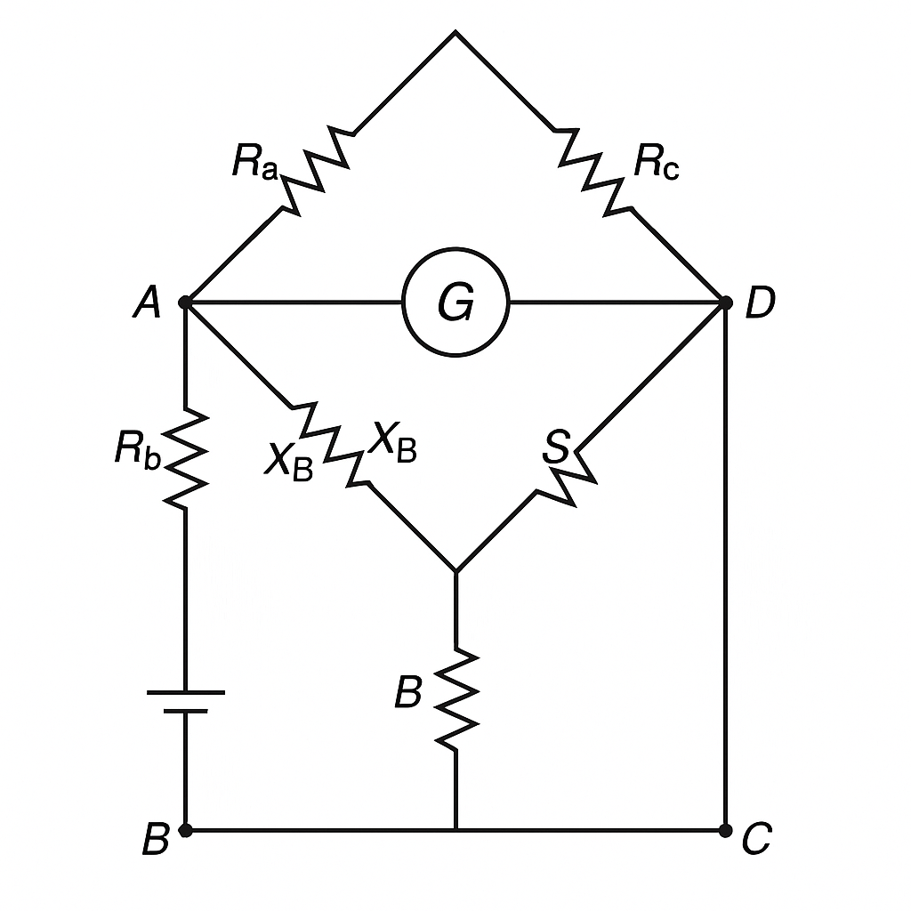
Kelvin double bridge electrical circuit diagram. Description is in the preceeding paragraphs.
Kelvin double bridge.

  • bridge network resistors: Ra, Rb, Rc, and S
  • lower portion of circuit: XB and the standard resistor B
  • null galvanometer: G

In the Kelvin double bridge circuit shown, the resistors Ra, Rb, Rc, and S form the bridge network that balances the ratio of known resistances against the unknown low resistance XB. The test current flows through the lower portion of the circuit, including XB and the standard resistor B, while the potential difference is sensed across the **bridge's diagonal arm** (the detector arm) between the upper nodes A and D. The point C serves as the common reference node for the current return path. The instrument labeled G is a null galvanometer—an extremely sensitive zero-center meter used to detect when no current flows between the two potential nodes, indicating that the bridge is balanced. When this condition is achieved, the ratio of the known resistances can be used to calculate the true value of XB, free from the influence of lead and contact resistances that would otherwise distort the result.


K Terms Index